


 Designer’s Notebook: What Designers Need to Know About Manufacturing, Part 2
 The Pulse: Drilling Down on Documentation
 Connect the Dots: Designing for Reality: Prioritizing Manufacturability
Intercept Unveils Enhancements to Pantheon Ink Resistor Technology
September 10, 2015 | Intercept Technology Inc.Estimated reading time: 2 minutes
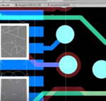
Intercept Technology Inc., a leading EDA software developer for PCB, RF and Hybrid Design solutions today announced powerful and leading-edge enhancements to Pantheon Ink Resistor functionality. In line with Intercept’s mission to provide the highest in advanced design technology, enhancements include the ability to create rectangular as well as complex ink resistor shapes parametrically on the fly during layout, or from information obtained from a schematic. Ink resistor components reside in the design database as parametric types, allowing for flexible modifications as needed at any point during the design process. And, new ink resistor functionality provides users with the ability to manipulate individual ink resistor layers, whether internal or external, creating powerful ink resistor modification capabilities. Defined parametric properties can be saved for use in any design, and users can auto-generate ink resistors based on given inks.
Ink resistor enhancements in Pantheon were built with intuitive graphics and dialogs for the easy setup, generation and modification of ink resistors. Users can create ink resistor shapes either from ink resistor calculation formulas or flexible dialog options as needed. The Ink Resistor Generator Dialog also includes a preview window that updates as ink resistor attributes are modified. And, easy-to-understand graphics help in the specification of such parameters as extensions for overglaze, placement and routing as well as net keepout outlines.
For ink resistor laser trim parameters, Pantheon capabilities provide full functionality with options for passive and functional trim, and additional options are available to specify static and/or dynamic trim clearances for placement and routing. Users can set resistor tolerances and trim percentages for flexibility in ink resistor creation.
“Enhancements to Pantheon’s ink resistor functionality combine the power of Pantheon’s PCB/Hybrid/RF design flow with the intuitive setup and modification of complex ink resistor shapes for the highest advancements in design layout and geometry creation,” said Dale Hanzelka, Director of Sales and Marketing at Intercept. “The resulting software solution provides users with the power to create the highest quality designs in a time of ever-advancing design needs.”
About Intercept
Intercept Technology Inc. is the leading supplier of PCB, RF, hybrid and high speed software solutions for the EDA industry. Intercept's software suite includes PCB schematic and layout design with simulation interfaces, design for manufacture (DFM) rules checking, library management, and 35+ database translators and interfaces that facilitate full environment migration as well as the completion of RF, hybrid, SiP, Analog, Digital, and Mixed-Signal designs. Additionally, Intercept's software solutions are scalable, serving small, medium and large sized companies.
Share on:


Suggested Items
iNEMI Packaging Tech Topic Series: Role of EDA in Advanced Semiconductor Packaging
04/26/2024 | iNEMIAdvanced semiconductor packaging with heterogenous integration has made on-package integration of multiple chips a crucial part of finding alternatives to transistor scaling. Historically, EDA tools for front-end and back-end design have evolved separately; however, design complexity and the increased number of die-to-die or die-to-substrate interconnections has led to the need for EDA tools that can support integration of overall design planning, implementation, and system analysis in a single cockpit.
Cadence, TSMC Collaborate on Wide-Ranging Innovations to Transform System and Semiconductor Design
04/25/2024 | Cadence Design SystemsCadence Design Systems, Inc. and TSMC have extended their longstanding collaboration by announcing a broad range of innovative technology advancements to accelerate design, including developments ranging from 3D-IC and advanced process nodes to design IP and photonics.
Ansys, TSMC Enable a Multiphysics Platform for Optics and Photonics, Addressing Needs of AI, HPC Silicon Systems
04/25/2024 | PRNewswireAnsys announced a collaboration with TSMC on multiphysics software for TSMC's Compact Universal Photonic Engines (COUPE). COUPE is a cutting-edge Silicon Photonics (SiPh) integration system and Co-Packaged Optics platform that mitigates coupling loss while significantly accelerating chip-to-chip and machine-to-machine communication.
Siemens’ Breakthrough Veloce CS Transforms Emulation and Prototyping with Three Novel Products
04/24/2024 | Siemens Digital Industries SoftwareSiemens Digital Industries Software launched the Veloce™ CS hardware-assisted verification and validation system. In a first for the EDA (Electronic Design Automation) industry, Veloce CS incorporates hardware emulation, enterprise prototyping and software prototyping and is built on two highly advanced integrated circuits (ICs) – Siemens’ new, purpose-built Crystal accelerator chip for emulation and the AMD Versal™ Premium VP1902 FPGA adaptive SoC (System-on-a-chip) for enterprise and software prototyping.
Listen Up! The Intricacies of PCB Drilling Detailed in New Podcast Episode
04/25/2024 | I-Connect007In episode 5 of the podcast series, On the Line With: Designing for Reality, Nolan Johnson and Matt Stevenson continue down the manufacturing process, this time focusing on the post-lamination drilling process for PCBs. Matt and Nolan delve into the intricacies of the PCB drilling process, highlighting the importance of hole quality, drill parameters, and design optimization to ensure smooth manufacturing. The conversation covers topics such as drill bit sizes, aspect ratios, vias, challenges in drilling, and ways to enhance efficiency in the drilling department.